 ESPEC North America, Inc. (Corporate office)
4141 Central Parkway
Hudsonville, MI 49426 USA ESPEC North America, Inc. (Colorado/Qualmark office)
12600 E. Smith Road
Aurora, CO 80011 USA
303-254-8800
Semiconductors sit at the heart of every modern technology breakthrough — from AI accelerators and high-performance computing to automotive electrification and advanced 3D packaging. As devices shrink, interconnects multiply, and heat loads intensify, the margin for error disappears. Reliability is no longer a late-stage checkbox; it is a competitive advantage.
In the race toward next-generation devices, even microscopic defects can trigger field failures, costly recalls, safety risks, or yield loss. The industry’s rapid transition toward chiplets, heterogeneous integration, 3D stacking, and ultra-fine redistribution layers only elevates this challenge.
That’s why environmental, electrical, and thermal testing must work hand in hand.
Microscopic defects do not always fail immediately. They emerge under stress:
Evaluating these mechanisms independently provides only part of the picture.
Electrical bias without environmental stress does not replicate real-world operating conditions. Environmental stress without live electrical monitoring delays failure detection.
When electrical measurement systems and environmental simulation operate in sync, failure modes become visible earlier and more clearly. Engineers can correlate temperature, humidity, pressure, vibration, and bias conditions directly with electrical degradation in real time.
That integration defines ESPEC’s semiconductor testing platform.
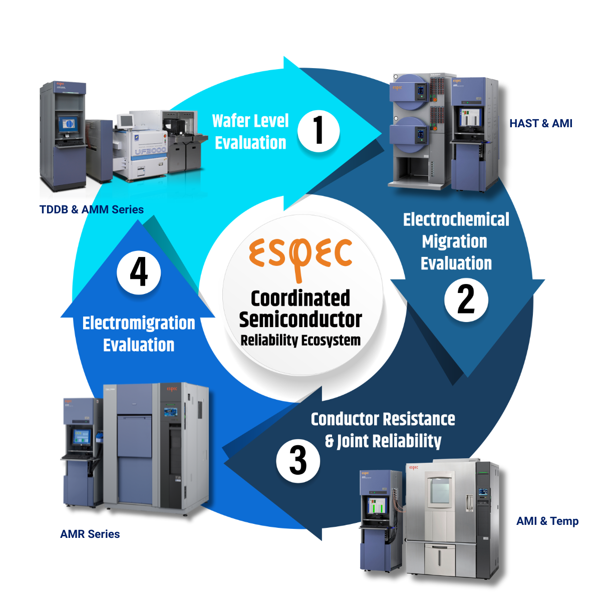
Semiconductor reliability is not built through a single test method. It is achieved through a coordinated evaluation strategy that spans wafer-level characterization, advanced packaging validation, accelerated environmental stress, and real-time electrical monitoring.
ESPEC’s semiconductor portfolio is structured to support this lifecycle — combining electrical evaluation systems with environmental simulation platforms to create a unified, repeatable, and standards-aligned testing environment.
From early defect detection at the wafer level to migration analysis, joint fatigue monitoring, electromigration evaluation, and high-acceleration stress screening, our solutions are engineered to measure how devices behave under real-world conditions — not just nominal ones.
The sections below outline how these systems work together to support modern semiconductor development and qualification.
Early-stage defect detection reduces downstream yield loss and reliability risk.
ESPEC supports wafer-level characterization and dielectric evaluation through advanced parametric and TDDB systems designed for leading-edge process development. These systems enable:
Integrated with precision temperature control where required, wafer-level evaluation helps engineering teams stabilize process performance before transitioning to advanced packaging and final qualification.
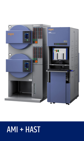
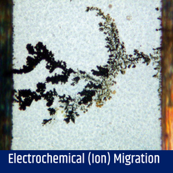
As redistribution layers narrow and substrate density increases, electrochemical migration and insulation degradation become primary reliability risks.
The AMI Series evaluates insulation resistance behavior and captures instantaneous migration events under controlled environmental stress. Key capabilities include:
When paired with:
AMI enables synchronized humidity, temperature, and bias application with real-time electrical monitoring.
This integration is critical for evaluating RDL insulation integrity, substrate migration behavior, and long-term package reliability under high-humidity stress conditions.
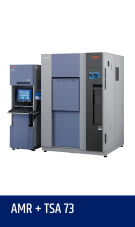
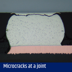
Advanced packaging architectures introduce mechanical stress between materials with mismatched coefficients of thermal expansion. Under rapid temperature transitions, microcracks can form at solder joints and interconnect interfaces.
The AMR Series continuously measures conductor resistance during accelerated thermal stress, allowing detection of intermittent or transient connection failures.
Core capabilities include:
Integrated with:
AMR correlates resistance fluctuation directly with thermal transition events. This is particularly valuable for FC-BGA, 2.xD / 3D packaging, TSV interconnects, and high-pin-count assemblies subject to aggressive cycling profiles.
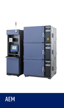
As current densities increase in shrinking interconnect geometries, electromigration becomes a dominant wear-out mechanism.
The AEM Series evaluates interconnect lifespan by applying controlled current density and elevated temperature conditions to accelerate degradation behavior.
When combined with precision temperature chambers, engineers can:
This approach strengthens long-term reliability modeling for advanced node and high-performance device applications.
Electrical measurement systems require stable, repeatable environmental control. Semiconductor reliability is proven under stress — not under nominal conditions.
ESPEC environmental platforms are engineered to replicate mission-critical operating environments while enabling synchronized electrical monitoring.
Operational extremes expose thermal fatigue, material expansion mismatch, and accelerated wear-out mechanisms.
Supported by:
These systems align with JEDEC temperature cycling requirements and aggressive transition profiles used for advanced packaging validation.
Moisture intrusion and electrochemical reactions drive corrosion, insulation degradation, and migration failure.
Supported by:
These platforms enable HHBT, pressure-based humidity testing, and high-temperature moisture stress aligned with JEITA and JEDEC standards.
Mechanical resonance and combined environmental stress can reveal latent defects that static testing cannot.
Supported by:
These platforms combine rapid thermal transitions and vibration to identify early-life defects and strengthen production screening strategies.
Devices deployed in aerospace, automotive, and extreme environments must withstand pressure variation and atmospheric changes.
Supported by:
These conditions can be simulated where application-specific validation requires pressure or reduced-atmosphere evaluation.
Together, these environmental systems form the foundation of semiconductor reliability testing — enabling engineers to apply controlled stress profiles that mirror real-world operating conditions while capturing electrical behavior in real time.
Semiconductor development cycles move quickly. Qualification timelines compress. Design iterations accelerate. Your testing infrastructure must keep pace.
ESPEC provides scalable environmental and semiconductor reliability solutions tailored to programs of every size:
As device architectures evolve, testing strategies must evolve with them. Our North American engineering and service teams work directly with customers to refine chamber configurations, optimize stress profiles, and ensure repeatable, standards-aligned evaluation.
From early-stage validation to full production screening, ESPEC systems are designed to scale alongside semiconductor innovation.
As via diameters in advanced semiconductor packaging substrates shrink to 50 μm and below, thermal stress introduces a growing reliability risk: cracking at the base of micro-vias. What makes this failure mode particularly difficult to catch is its behavior under static conditions — weak micro-vias often remain electrically connected when temperature is held constant, masking the defect entirely.
To evaluate this mechanism, a substrate board with a daisy chain configuration (via size: 50–70 μm, double-sided 3-layer structure) was subjected to temperature cycle testing from -55°C to +150°C per JEDEC No. 22-A104E, using an ESPEC TSA thermal shock chamber paired with the AMR-280 Conductor Resistance Evaluation System.
Continuous resistance monitoring during thermal transitions — not just at steady-state intervals — revealed the failure signature: conductor resistance increased precisely during temperature changes, then recovered as conditions stabilized. Without real-time monitoring through the full thermal cycle, this intermittent behavior would have gone undetected.
This is the diagnostic capability that matters in advanced packaging validation. Spot checks and static measurements leave gaps. Continuous, synchronized electrical monitoring during environmental stress closes them.
Semiconductor reliability demands precision, repeatability, and technical depth. Over decades of environmental simulation and semiconductor evaluation experience, ESPEC has become a trusted partner to global manufacturers, advanced packaging innovators, and high-performance device developers.
Our customers rely on ESPEC for:
From early wafer-level validation to advanced packaging qualification and production screening, ESPEC systems are engineered to support measurable, defensible reliability outcomes.
Reliability is not assumed. It is validated.
Q: Can ESPEC customize test chambers for unique semiconductor applications?
Yes. Environmental platforms and integrated system configurations can be tailored to support specialized device geometries, packaging structures, and qualification requirements. Connect with our engineering team to discuss your specific device or process constraints.
Q: What is the typical lead time for equipment delivery or rental?
Lead times vary by system type and configuration. Quick-ship and rental chamber options are available to support urgent qualification or pilot builds. Contact us for current availability and configuration guidance.
Q: Does ESPEC provide compliance support for global semiconductor standards?
Yes. ESPEC systems support testing aligned with JEITA, JEDEC, IEC, IPC, automotive, and mission-critical reliability standards. Our engineering teams assist customers in aligning stress profiles and validation procedures with applicable requirements. Schedule a technical consultation to review your compliance objectives.
Q: How is ongoing service and calibration handled?
ESPEC provides global service and technical support, including preventive maintenance programs, calibration services, and application guidance to maintain system accuracy and long-term performance. Reach out to coordinate service planning or lifecycle support for your systems.
Q: Can I request a demo or technical consultation?
Yes. Technical consultations, system evaluations, and application discussions are available to determine the optimal configuration for your semiconductor reliability program. Request a consultation to begin evaluating your requirements.
Semiconductor reliability requires more than equipment — it requires a testing strategy built for how devices actually fail. Whether you are qualifying a new design, validating an advanced packaging architecture, or scaling production screening, our engineering team is ready to help you build the right evaluation approach.
Contact us to schedule a technical consultation, request a system configuration, or discuss your qualification requirements.
Reliability is not assumed. It is validated.
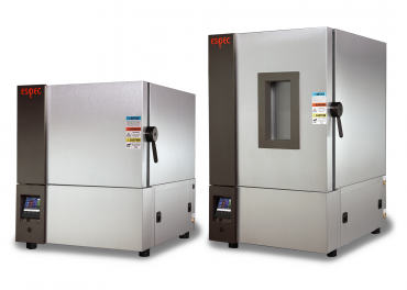
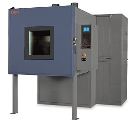
Twenty different benchtop models
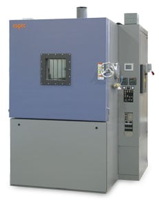
Industrial-quality chambers for combination testing with vibration systems
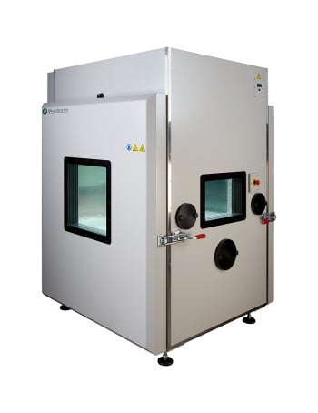
Simultaneous testing of temperature and low-pressure altitude conditions
Get your Qualmark or other brand HALT chamber upgraded to a modern control and vibration system.
ESPEC North America, Inc. (Corporate office)